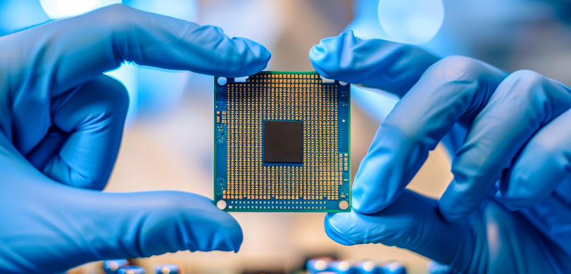
India is entering a transformational phase in its technological development. The semiconductor sector is growing rapidly and offers a rare window of opportunity for engineers, fresh graduates and professionals looking to build meaningful careers. Enrolling in a semiconductor program in India now will put you ahead in a field where demand, investment and skill-gap align to create strong
advantages.
India’s Semiconductor Ecosystem: Growth, Opportunity and the Talent Gap
The government of India has made semiconductor manufacturing a national priority by launching the India Semiconductor Mission (ISM), which intends to create an ecosystem not only for fabs but also for ATMP units, design, research, and skilled workforce development. This national ambition takes shape in the form of ₹ 76,000 crore commitment under the semiconductor incentive scheme to attract both global and domestic players. So far, India has given the green light to a handful of large-scale projects like Micron ATMP facility in Gujarat (USD 2.75 billion) and has received major proposals by Tata Electronics for fabs and OSAT units, Foxconn for semiconductor facilities, and significant investments by AMD, Lam Research and Applied Materials in design, R&D, and training.
In the words of the Honourable Prime Minister, Shri Narendra Modi
“India will not miss the semiconductor bus this time.”
These moves propel India’s transition from a consumption-driven electronics market to a viable manufacturing and design hub. Several recent reports set the tone for the magnitude of the talent gap. According to Team Lease Degree Apprenticeship, the semiconductor industry in India will need 250,000 to 300,000 professionals in semiconductor R&D, design, manufacturing, and packaging by 2027. As per Randstad, hiring needs in the Indian semiconductor industry were up by 25-30% in 2024, with 40,000-50,000 roles, and overall demand would reach 800,000 to 1 million jobs in the next five years.
Considering the growth potential of the sector and the sizable investments being made, this is a now-or-never time.
Students who enrol in a dedicated semiconductor manufacturing program will graduate when demand is at its highest, staying ahead of the curve.
Career Growth and Salary Potential in Semiconductor Manufacturing
As a vital industry, the semiconductor sector is quite specialised, and professionals equipped with practical skills and knowledge in the field would generally enjoy a quicker career advancement than typical engineering graduates. There are many entry-level job opportunities including the likes of Process Engineers, Equipment Engineers, Yield Analysts, Test Engineers, Packaging Engineers, or Reliability Engineers.
Fresh graduates with the relevant skills may get a salary of between ₹6-12 lakhs per year, and as per The Times of India, Freshers’ salaries in semiconductor fabs and ATMP units are among the highest for engineering graduates entering high-tech manufacturing. Mid-career engineers (4-10 years) working in high-growth fabs or packaging units can make ₹25-35 lakhs or more, depending on the role, company, and location. Senior positions in design, verification, or fab operations may provide wages that are significantly higher than these.
With rising demand, the expansion of India’s semiconductor ecosystem, and the convergence of capabilities in manufacturing, design, and packaging, upskilling in this sector now will set the person on a very attractive career path. Benefits include high initial salaries, swift skill acquisition, international experience, and the availability of multiple career routes.
Why a Specialised Semiconductor Program Makes a Real Difference and Why Students Should Pursue it?
While generic engineering or electronics degrees provide broad theoretical foundations, a specialised semiconductor manufacturing program develops specific domain skills that the industry requires. Students must think of such program because:
- The semiconductor sector in India is expanding at a phenomenal speed, which is facilitated by a strong policy, large investments, and increasing global partnerships.
- The huge talent gap offers those who enter the sector early a strategic advantage.
- Wages in semiconductor jobs are much higher than in many IT or general engineering jobs.
- A specialised program will speed up the students’ industry readiness, ensuring that they are job-ready from day one.
- The convergence of fabrication, design, packaging, and test ensures the longevity of the industry and multiple career paths.
Courses such as the Master in Semiconductor Manufacturing Technology and Management at NAMTECH prepare students for the high-growth semiconductor industry. The program offers learning from expert faculty, hands-on training, advanced and cutting-edge labs, access to the latest process equipment and direct industry interaction with leading semiconductor organisations such as Micron, FESTO and Rockwell Automation.
How Students Should Evaluate a Semiconductor Program?
With numerous program emerging in the semiconductor field, students require a definite plan to distinguish genuinely industry-oriented training from generic courses. An excellent program in semiconductors should point to three major aspects: laboratories, faculty, and placement. Students must evaluate each pillar in depth.
1. Laboratories
An impressive laboratory is the heart of a good semiconductor program. Students should verify that:
- The clean rooms are operational and have controlled environments
- Wafer fabrication includes the following procedures: lithography, deposition, etching, and CMP.
- Packing and testing facilities are available
- The tools used for simulation and design are the same as those used in the industry
- Students have access to real instruments and not just theoretical demonstrations
Hands-on labs ensure students learn how processes work, how they can handle the tools safely, and how they can build their confidence for fab or ATMP roles.
2. Faculty Expertise and Industry Involvement
The better the faculty, the deeper the learning. Students should evaluate that:
- Faculty are not just the employees of fabs, ATMP units, or research labs, but they also have direct experience there.
- Faculty members are industry-certified or do research work in semiconductor processes.
- Fab engineers, tool specialists, and industry leaders come and give guest lectures.
- Semiconductor companies oversee the curriculum or provide advisory support.
Good and strong faculty members play a great role in making learning always updated, relevant, and linked to the present industry needs.
3. Placement Support and Industry Linkages
Program must show obvious routes to getting a job. Students are expected to verify that:
- Fabs, ATMP units, OSAT companies, and design houses have active partnerships. Faculty members are industry-certified or do research work in semiconductor processes.
- Internship opportunities are an integral part of the program.
- Industry-sponsored live projects or capstone assignments
- Historical placement data, recruiter names, and alumni career paths
Such an assessment enables a student to pick a program that will really prepare them for a career in semiconductors rather than just giving surface-level courses.
If you are serious about a career in cutting-edge technology manufacturing, enrol in a focused semiconductor manufacturing program now. Doing so positions you to join a high-growth industry, start strong and progress fast.
It’s time your higher education actually takes you higher!

Designation : Sr. Associate Director
04 December, 2025


