For most of this decade, India’s semiconductor ambitions lived in press releases. Cabinet approvals, MoUs at investment summits, announced partnerships that took years to move. Engineers were right to be skeptical.
2026 is different. PM Modi inaugurated Micron Technology’s ATMP facility in Sanand, Gujarat in February 2026, and the Kaynes Semicon plant in Sanand in March 2026. In April 2026, groundbreaking happened for India’s first advanced 3D semiconductor packaging unit in Odisha. In May 2026, Rajasthan got its first semiconductor plant, and the Cabinet approved two more semiconductor manufacturing units with cumulative investment exceeding ₹3,900 crore. These are not announcements. These are operational facilities.
If you are an engineering graduate deciding what to do with the next five years of your career, this is the context you are working in.
From Policy to Production: What’s Actually Been Built
The India Semiconductor Mission launched in 2021 with a ₹76,000 crore incentive framework and a mandate to build a domestic chip ecosystem from scratch. As of mid-2026, 10 projects totalling ₹1.60 lakh crore are approved across six states, spanning silicon fabrication, compound semiconductor fabs, and advanced packaging facilities.

The anchor investments: Tata Electronics is building India’s first commercial front-end wafer fab in Dholera, Gujarat, in partnership with Taiwan’s PSMC, targeting 28nm–110nm chips with first production by end of 2026. Tata’s OSAT facility in Jagiroad, Assam, capable of packaging up to 48 million chips per day, is under construction. Micron’s ATMP plant in Sanand is operational. Kaynes Semicon — which shipped India’s first commercially packaged multi-chip modules to a US client in October 2025 — is now an inaugurated facility. ISM 2.0, announced in the Union Budget 2026–27, shifts focus to the next layer: semiconductor equipment and materials, full-stack Indian chip design IP, and building the supply chains that surround a fab ecosystem.
One clarification worth making: TSMC is not building a fab in India. The surge in searches for “TSMC jobs in India” reflects the company’s growing design-ecosystem presence — Indian firms joining TSMC’s design center network, and TSMC recruiting Indian engineers for roles based in Taiwan. That is a real opportunity, but it is not a manufacturing plant on Indian soil.
The Career Map Is Wider Than You Think
Most content written about semiconductor careers in India defaults to chip design in Bangalore. That is one part of the picture — and it was nearly the whole picture until recently. It isn’t anymore.
Three forces converged to change this: substantial committed capital under the India Semiconductor Mission, fab and ATMP commitments from Tata Electronics, Micron, and Kaynes, and diversification pressure on global semiconductor companies to reduce concentration risk in Taiwan and Korea. The result is a career landscape that now spans design and manufacturing, and runs across Gujarat, Assam, Odisha, Rajasthan, Uttar Pradesh, and the south.
The roles being created fall into distinct clusters. Chip design — RTL, physical design, verification, DFT, analog — remains concentrated in Bengaluru, Hyderabad, and Chennai, and is where most ECE graduates aim. But fab process engineering (lithography, etch, deposition, yield), test and packaging engineering, equipment engineering, and quality and reliability engineering are all opening at scale as the new plants ramp up. The sector demands a highly diverse mix of skills: electronics and VLSI engineers for circuit design and verification, computer science engineers for EDA software, mechatronics engineers for cleanroom robotics and automated systems, and chemical and materials engineers for etching, gas deployment, and silicon wafer purification.
This matters for how you think about your own background. ECE, EEE, CSE, mechanical, chemical, materials — the semiconductor industry has a use for all of them. The question is which part of the stack you want to work on.
What the Market Is Paying in 2026
Salaries are tiered, and the gap between tiers is wide. Fresher semiconductor engineers earn between ₹4.8 LPA and ₹20 LPA, with advanced and niche positions — particularly in chip design and AI-chip architecture — paying considerably higher. At Tier-1 product companies (NVIDIA, Texas Instruments, Intel, Qualcomm), fresher CTCs for design roles are consistently reported in the ₹17–28 LPA range. EDA firms like Synopsys and Cadence sit in the ₹12–25 LPA band. Indian services and manufacturing firms start lower but offer faster entry into the sector.
The more important data point is trajectory. Engineers with three to five years of experience typically earn ₹18–26 LPA, with the highest-grade MNC semiconductor engineers reaching ₹40–60 LPA or more including stock and bonuses. Semiconductor careers command a 25–35% premium over mainstream IT at equivalent experience levels, and that gap widens with specialization.
The highest-premium niches: UVM verification on complex IPs, advanced-node physical design (5nm and below), DFT for memory and ATPG, and analog/mixed-signal — the smallest talent pool and the highest paid.
The Skills Gap Is the Real Opportunity
Meeting the growth of India’s semiconductor sector requires upskilling and reskilling 500,000 people every year. India graduates roughly 600,000 electronics engineers annually, but only a fraction are immediately usable by chip companies and fabs. The gap is not about intelligence or aptitude. It is about what a standard B.Tech curriculum teaches versus what an employer actually needs on day one.
A typical ECE program covers CMOS fundamentals, sees a Verilog module in a lab session, and moves on. Employers need engineers who can write synthesizable RTL, run it through EDA tools, close timing, write a UVM testbench, understand DRC and LVS, and script in Python or Tcl. The gap is practical, not conceptual — and it is closeable in four to six months of focused work if you choose the right tools and actually build something defensible.
That gap is your entry point. The engineers who close it before graduation, or immediately after, are the ones getting the offers that make the salary tables above look real rather than aspirational.

The Techno-Manager: The Profile India’s Fabs Are Hungry For
There is a career profile that barely existed in India three years ago and is now actively being sought by every major fab and OSAT coming online: the engineer who understands semiconductor technology deeply enough to make production decisions, and understands manufacturing operations, supply chains, and business tradeoffs well enough to lead them.
Running a fab or an OSAT is not the same as designing a chip. It requires managing yield, coordinating with equipment vendors, optimizing throughput, handling procurement, and making decisions that sit at the intersection of engineering and business. As India’s manufacturing investments build the missing parts of the semiconductor stack, demand is surging for manufacturing-operations leaders skilled in high-precision production, yield, testing, and supply-chain management. India currently has very few people trained for this.
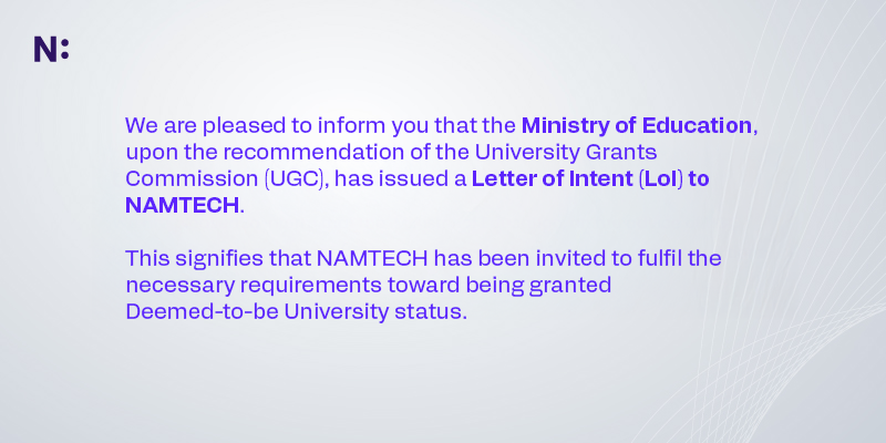
Programs like NAMTECH’s Master in Semiconductor Manufacturing Technology and Management — located at the IIT Gandhinagar Research Park, adjacent to the Sanand and Dholera clusters — are explicitly built for this profile. The curriculum covers IC fabrication, assembly and packaging, AI in semiconductors, plant engineering, and supply chain alongside the core semiconductor science. Industry partners include Micron, CG Power, Kaynes, and Tata Electronics — the same companies building the plants. The first batch begins August 2026, with an ISM–NAMTECH collaboration MoU in place to develop the talent pipeline.
This is the manufacturing-leadership track. It is distinct from chip design, it is less crowded, and it has a direct line to the facilities being built right now.
Should You Do a Master’s? An Honest Answer
For chip design roles at Tier-1 product companies, an M.Tech — particularly from IIT, NIT, IISc, or BITS — meaningfully improves your entry package and opens doors that a B.Tech alone will struggle to open at those firms. If architecture, research, or the design track at a company like NVIDIA or Intel is the goal, M.Tech is worth the two years.
For everything else, the calculation is more open. The semiconductor sector is broad enough that a B.Tech with demonstrable job-ready skills — real EDA-tool experience, a portfolio project, working knowledge of synthesis and timing — can land design, verification, test, and manufacturing roles without a postgraduate degree. The new manufacturing and OSAT roles being created in Gujarat and Assam are explicitly accessible to B.Tech graduates who understand the process side.
The honest answer is: it depends on which part of the sector you are targeting. What does not depend on the answer is the skills gap. Whether you do a master’s or not, the engineers winning in this market are the ones who have closed the gap between what their curriculum taught them and what the industry actually runs on.
India’s semiconductor moment is not a projection anymore. The plants are operational, the mission has a second phase, and the hiring is real. The question is whether you are ready to walk into it.

02 July, 2026