Announcements
The semiconductor industry in India is in the middle of a real transformation — not a projected one. Government initiatives like the India Semiconductor Mission, rising domestic demand, and global supply chain diversification are creating engineering roles that did not exist at scale three years ago. For B.Tech students aiming to enter this field, understanding what those roles actually are, what they require, and who is doing the hiring matters far more than generic career advice.
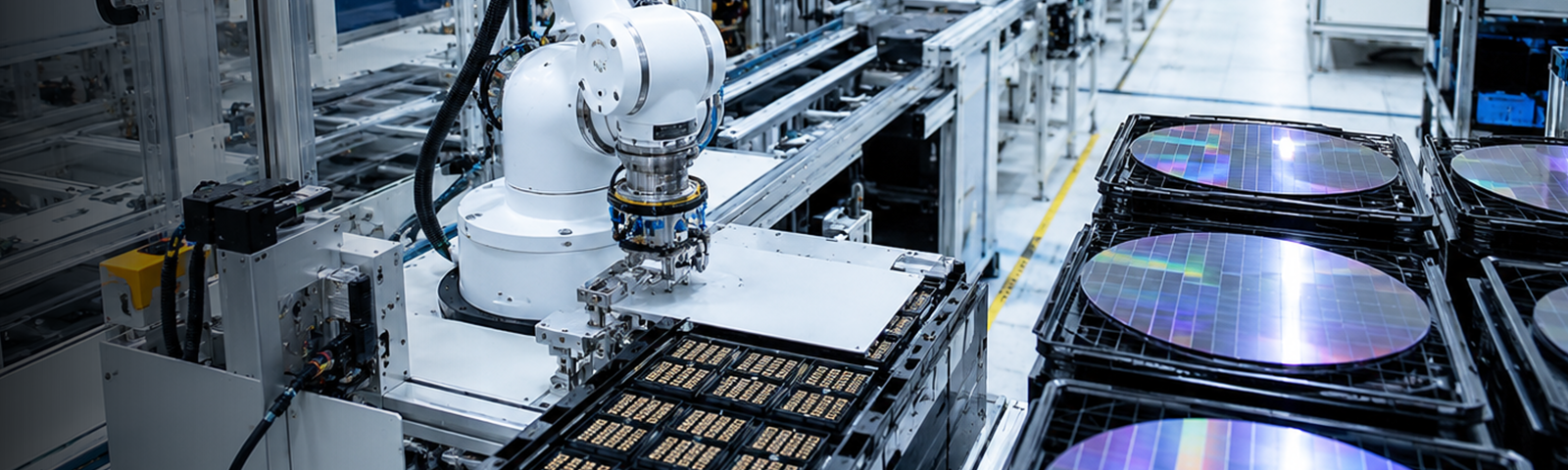
Roles in Indian Chip Fabrication Plants
Chip fabs in India hire for roles that are technical, process-driven, and demanding. These are not assembly-line positions — they require rigorous training, deep engineering fundamentals, and in many cases clean room certification.
Process Engineer: Focuses on the core steps of semiconductor manufacturing — photolithography, etching, doping, and metallization. Requires a strong understanding of chemical and physical fabrication processes and is typically the most technically demanding role in a fab.
Equipment Maintenance Engineer: Maintains the precision tools that keep a fab running. Semiconductor equipment is extraordinarily expensive and sensitive; minimizing downtime and maintaining process stability are the job. Requires mechanical and electrical engineering depth plus vendor-specific training.
Quality Assurance and Test Engineer: Responsible for product inspection, electrical testing, and data analytics to maintain high yields. This role sits at the intersection of engineering and data interpretation and is growing rapidly as new OSAT facilities ramp up in India.
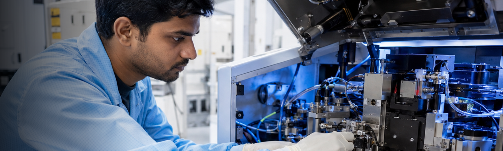
Chip Design and Verification Roles
India’s semiconductor design houses and R&D centers focus heavily on the design and verification of integrated circuits. These roles concentrate in Bengaluru, Hyderabad, and Chennai and require strong ECE or EEE foundations.
VLSI Design Engineer: Designs chip circuitry based on specifications using EDA tools. Proficiency in Verilog/SystemVerilog and knowledge of digital and analog circuit design are standard requirements.
Verification Engineer: Creates testbenches and verifies chip functionality through simulation before fabrication. Increasingly in demand as design complexity grows; UVM methodology is the current industry standard.
Physical Design Engineer: Converts logical design into layouts optimized for performance and power. One of the highest-premium specializations in the sector.

Skills That Actually Get You Hired
Indian employers consistently flag the same gaps. The theory is not the problem — most B.Tech programs cover device physics and digital design adequately. The problem is practical depth.
EDA tool fluency: Familiarity with Cadence, Synopsys, or Mentor Graphics is a real differentiator. Knowing what the tools do in theory is not the same as having run a design through one.
Cleanroom protocol: For fab roles, knowledge of contamination control and safety procedures is non-negotiable. Employers will not train this from scratch.
Programming and scripting: Python and TCL scripting for automation in design and testing workflows are expected, not optional.
The minimum qualification is a B.Tech in Electronics, Electrical, or related engineering. An M.Tech or specialized postgraduate program in VLSI or semiconductor technology meaningfully improves prospects for design and R&D roles, particularly at Tier-1 product companies.
What the India Semiconductor Mission Is Actually Creating
The India Semiconductor Mission provides fiscal support of up to 50% of project cost for approved semiconductor facilities. As of December 2025, 10 projects with a total investment of Rs.1.60 lakh crore have been approved across six states. Micron’s ATMP facility in Sanand, Gujarat is operational. Kaynes Semicon’s OSAT unit in Sanand was inaugurated in March 2026. Tata Electronics is building India’s first commercial front-end wafer fab in Dholera, Gujarat, with first production targeted by end of 2026. Tata’s OSAT facility in Jagiroad, Assam is under construction.
These are not future projections — they are current build-outs creating process engineering, equipment, test and packaging, and manufacturing operations roles that did not exist in India at this scale before.
Government skill development programs including Chips to Startup (C2S) and the SMART Lab initiative are running in parallel, with NIELIT providing certificate and diploma courses in embedded systems and semiconductor technology, and IITs and IISc expanding research lab capacity in VLSI and fabrication.
The Skills Gap Is the Actual Bottleneck
Despite graduating hundreds of thousands of electronics engineers annually, India faces a genuine skills gap in semiconductor-specific domain knowledge. Employers report that standard B.Tech curricula teach device physics and basic Verilog but fall short on EDA tool workflows, verification methodology, clean room practice, and process engineering depth. This gap is closeable — but it requires deliberate effort beyond the degree.
For students targeting the manufacturing and operations side of the semiconductor industry — process engineering, yield management, packaging, supply chain — NAMTECH’s Master in Semiconductor Manufacturing Technology and Management offers a direct route. The two-year residential program, based at the IIT Gandhinagar Research Park adjacent to the Gujarat semiconductor cluster, covers IC fabrication, assembly and packaging, AI in semiconductor manufacturing, plant engineering, and supply chain management. Industry partners include Micron, CG Power, Kaynes, and Tata Electronics — the same companies building India’s fabs and OSATs. An ISM-NAMTECH collaboration MoU is in place to develop the talent pipeline for these facilities. The first batch commences August 2026.
For students targeting chip design and verification roles, the path runs through focused EDA tool training, a defensible portfolio project, and ideally an M.Tech from IIT, NIT, IISc, or BITS for Tier-1 product company access.
Where the Opportunities Actually Are
Rising manufacturing ecosystem: New fabs and OSAT units in Gujarat, Assam, Odisha, Rajasthan, and Uttar Pradesh are creating process, equipment, and manufacturing operations roles at scale.
Design and R&D centers: Indian operations of Qualcomm, Intel, Texas Instruments, NVIDIA, Applied Materials, and Lam Research are expanding design and engineering teams.
Ancillary sector: Semiconductor equipment manufacturing, testing labs, materials suppliers, and EDA services are all growing alongside the primary fabs.
The honest summary: India is building a semiconductor industry that needs engineers across the full stack — design, verification, fab process, packaging, equipment, and manufacturing leadership. The gap between what the average B.Tech produces and what employers need is real, but it is not permanent. Close it deliberately, and the timing has never been better.

02 September, 2026